We can try and prove the function of The Not Schmitt Gate as Clock Generator with following this Circuit Diagram in ELECTRONIC WORK BENCH
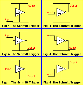
And these are several information about THE NOT SCHMITT TRIGGER


Schmitt Trigger Characteristic:

The output is HIGH until the input rises to 66% of rail voltage.
The output goes LOW when the input goes above 66%.
The output remains HIGH until the input fall to 33%.
The output goes LOW when the input goes above 66%.
The output remains HIGH until the input fall to 33%.
A Schmitt Trigger gate can be wired as an oscillator, delay, inverter (and other functions, depending on the surrounding components).
Fig: 5 shows the Schmitt Trigger wired as an oscillator, delay and inverter:
Fig: 5 shows the Schmitt Trigger wired as an oscillator, delay and inverter:

Each of the 6 gates in the 74c14 can be used to create a separate "building block" and this gives the chip a wide range of capabilities.
Schmitt Inverter Waveform Generator

This simple waveform generator circuit consists of a single TTL 74LS14 Schmitt inverter logic gate
with a capacitor, C connected between its input terminal and ground, ( 0v ) and the positive feedback required for the circuit to oscillate being provided by the feedback resistor, R.
with a capacitor, C connected between its input terminal and ground, ( 0v ) and the positive feedback required for the circuit to oscillate being provided by the feedback resistor, R.
So how does it work?. Assume that the charge across the capacitors plates is below the Schmitt’s lower threshold level of 0.8 volt (Datasheet value). This therefore makes the input to the inverter at a logic “0” level resulting in a logic “1” output level (inverter principals).
One side of the resistor R is now connected to the logic “1” level ( +5V ) output while the other side of the resistor is connected to the capacitor, C which is at a logic “0” level (0.8v or below). The capacitor now starts to charge up in a positive direction through the resistor at a rate determined by the RCtime constant of the combination.
When the charge across the capacitor reaches the 1.6 volt upper threshold level of the Schmitt trigger (datasheet value) the output from the Schmitt inverter rapidly changes from a logic level “1” to a logic level “0” state and the current flowing through the resistor changes direction.
This change now causes the capacitor that was originally charging up through the resistor, R to begin to discharge itself back through the same resistor until the charge across the capacitors plates reaches the lower threshold level of 0.8 volts and the inverters output switches state again with the cycle repeating itself over and over again as long as the supply voltage is present.
So the capacitor, C is constantly charging and discharging itself during each cycle between the inputs upper and lower threshold levels of the Schmitt inverter producing a logic level “1” or a logic level “0” at the inverters output. However, the output waveform is not symmetrical producing a duty cycle of about 33% or 1/3 as the mark-to-space ratio between “HIGH” and “LOW” is 1:2 respectively due to the input gate characteristics of the TTL inverter.
The value of the feedback resistor, ( R ) MUST also be kept low to below 1kΩ for the circuit to oscillate correctly, 220R to 470R is good, and by varying the value of the capacitor, C to vary the frequency. Also at high frequency levels the output waveform changes shape from a square shaped waveform to a trapezoidal shaped waveform as the input characteristics of the TTL gate are affected by the rapid charging and discharging of the capacitor. The frequency of oscillation for Schmitt Waveform Generators is therefore given as:

Tidak ada komentar:
Posting Komentar